The scrap material produced due to diamond wire (DW) failure certainly varies depending on the diamond wire, lubricant, and operating conditions. For an optimized process with only 2% of scrap material being produced and a single wafer valued at 0.35$/W, this would be the equivalent of $1M worth of scrap silicon for a 200MW wafering line. It is evident that an in-line metrology solution that can help reduce silicon waste due to DW breakage would be very valuable and provide up to a $1M/year in savings for 200MW wafering line.
Currently, wafer producers are exploring high resolution optical imaging techniques to assess the quality of diamond wires. The following are disadvantages of this approach:
- Optics provide only surface diagnostics, while the wearing stage also contributes to the sub-surface layers (Ni, Cu),
- It is not realistic to monitor optically the entire length of a DW in the cutting stage,
- Automatic algorithm for optical inspection is highly complicated
- Ingot cutting process creates a lot of residuals harmful for high-resolution optic hardware, which would require cleaning and maintenance of the tool.
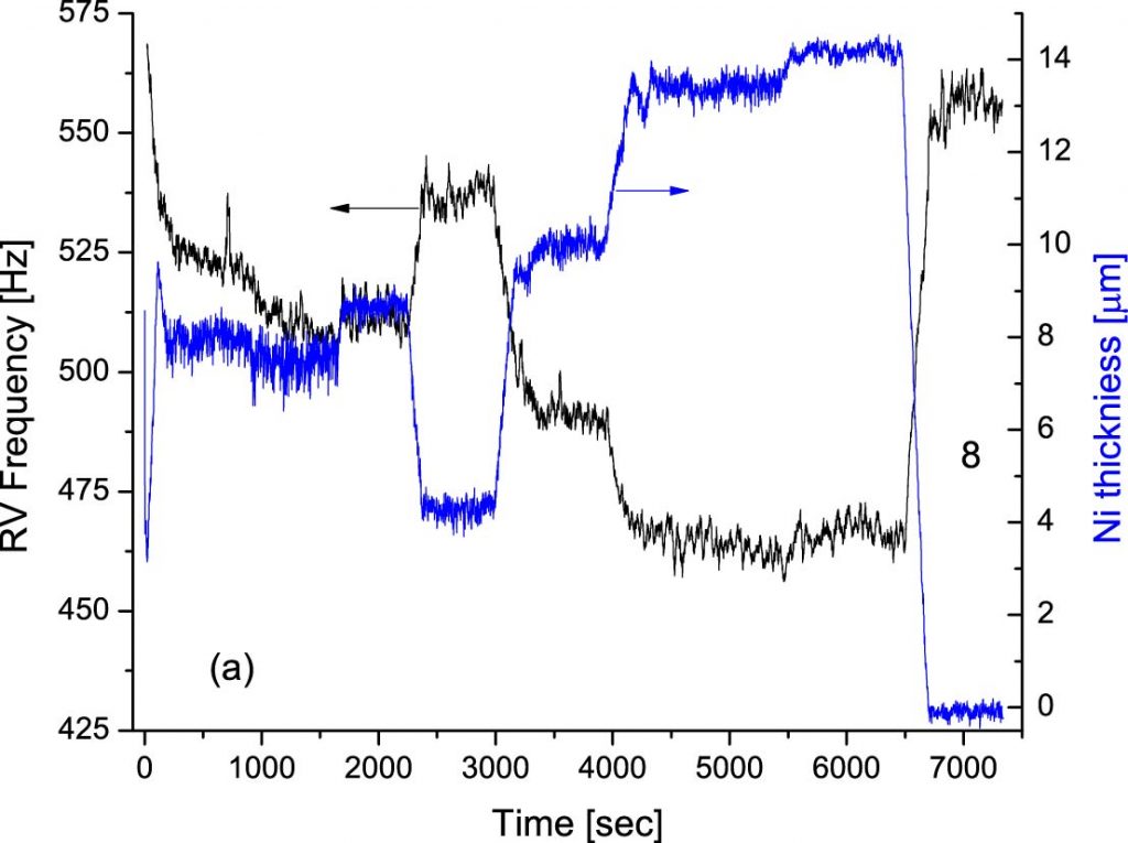
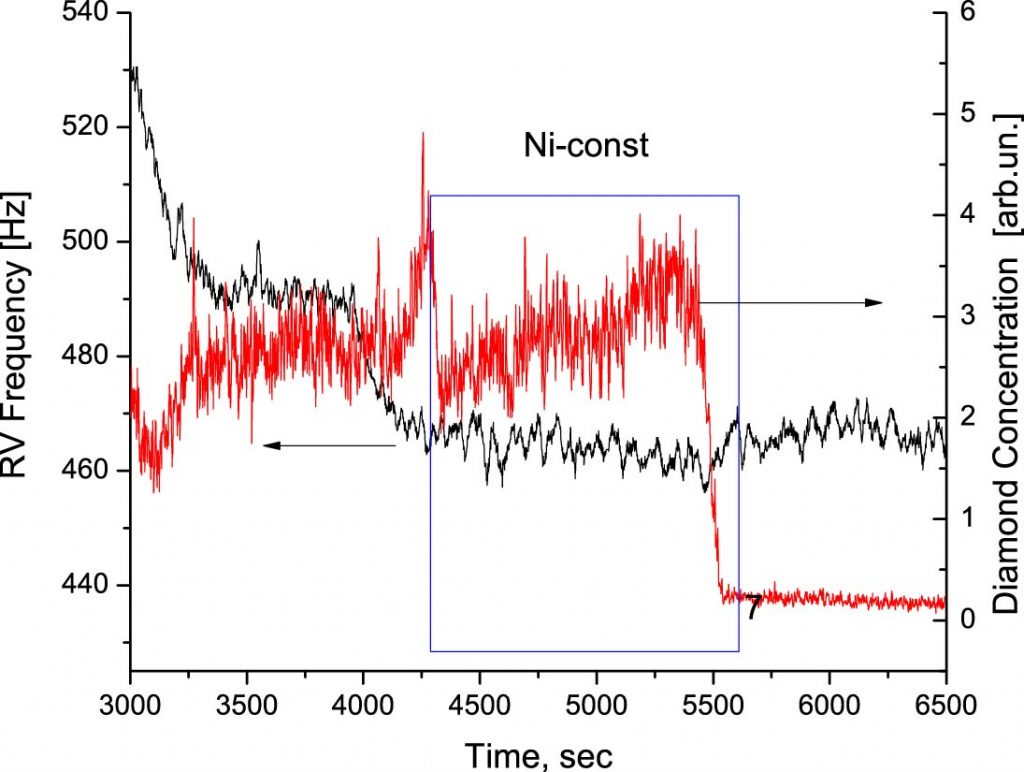
The overall objective of the current project is to develop a new metrology to inspect—in real-time—the quality of the Diamond Wire used for crystalline silicon wafering. The proposed metrology will ensure the complete inspection of the wire during the production phase. In addition, recent lab test results indicate that the metrology key metrics are independent of wire speed; therefore, scaling to higher cutting speed is expected to be straightforward, which is not the case for optical methods because of complex and time consuming image processing algorithms.
Years of Research: 2013-2017
Sponsored by: U.S. Department of Energy (SunShot PVMI and Incubator 11)
Prototype 1: Stationary Wire (November 2013)
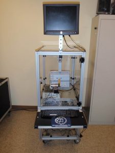
Prototype 2: Moving Wire (July 2014)
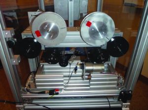
Prototype 3: Portable, Non-contact Sensor (July 2015)
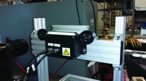
Field Testing Results for Diamond Wire Pilot Production Line
